
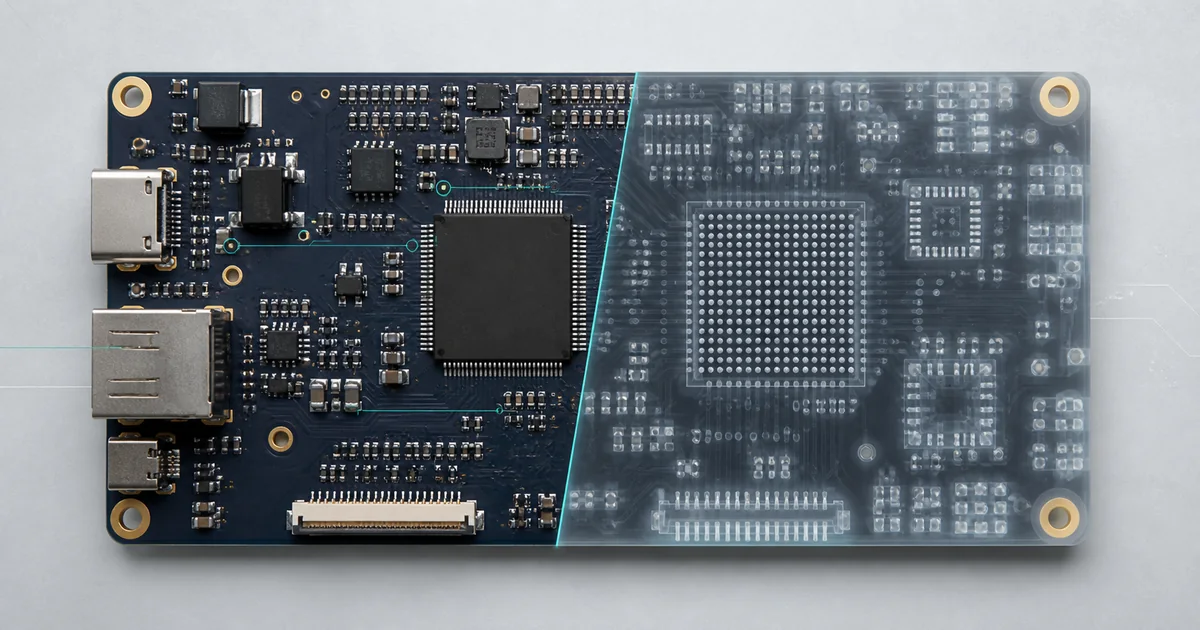
AOI is suited to optically visible placement and solder conditions. X-ray can provide evidence about solder structures hidden beneath packages such as BGAs and QFNs. Neither replaces defined electrical or functional testing.
Start with the inspection question
Choose evidence from the feature location and suspected condition. A visible polarity mark and a hidden BGA solder connection are not the same inspection problem, and image-based inspection does not replace electrical or functional testing.
AOI vs X-ray Inspection Coverage Matrix
| Feature or question | AOI contribution | X-ray contribution | Important limit |
|---|---|---|---|
| Presence, position and visible polarity | Strong when features and markings are optically accessible | Usually not the primary method | Marking quality, occlusion and programmed criteria affect evidence |
| Visible gull-wing or exposed solder joints | Can measure/classify visible geometry and surface conditions | May add internal density evidence when justified | Neither image alone proves electrical function |
| BGA hidden joints | Cannot directly see joints beneath the package | Can show joint pattern, bridging indicators and internal solder-density differences | Interpretation and acceptance criteria must be defined |
| QFN / bottom-terminated thermal pad | Can inspect visible package position and exposed perimeter features | Can provide hidden solder-distribution/voiding evidence | No universal voiding percentage applies to every design |
| Internal barrel, trace or component condition | Limited to visible surface evidence | Capability depends on geometry, view and system | Use a method matched to the exact suspected condition |
| Continuity and shorts | May find visible causes | May show physical indicators | Use flying probe/ICT or another electrical method for electrical evidence |
| Product behavior | No | No | Requires a defined functional test or system-level verification |
BGA / QFN review checklist
- Identify package construction, hidden-joint area and the failure question.
- Provide the assembly drawing, package datasheet and relevant pad/thermal design context.
- Define required views or evidence before the build where possible.
- Name the contractual acceptance source and revision; do not invent a percentage after imaging.
- Record image identity, board revision, component designator and reviewer disposition.
- Escalate ambiguous evidence rather than treating one image as a diagnosis.
What the image cannot prove
AOI and X-ray can support workmanship decisions, but they do not prove firmware, analog performance, timing, RF behavior or complete product function. Combine inspection with the electrical and functional evidence required by the product risk.
Inspection availability, method, coverage, and deliverables depend on the board and selected manufacturing partner; confirm them for the actual assembly.
Sources and scope
- Omron automated inspection systems — official AOI/AXI capability context.
- Omron AXI white paper — hidden-joint motivation and X-ray inspection context.
- IPC document revision table — verify the current revision of any contractually selected IPC document.
Continue the decision path
Use the related service and engineering guides to define the project scope before quotation or release.
Need a project-specific review?
Share the released files, quantity, open decisions and required evidence.