
IoT Sensor PCB Assembly: Component, Power and Testing Considerations
Resolve module integration, sensor interfaces, power states, firmware identity and validation evidence before releasing an IoT sensor build.
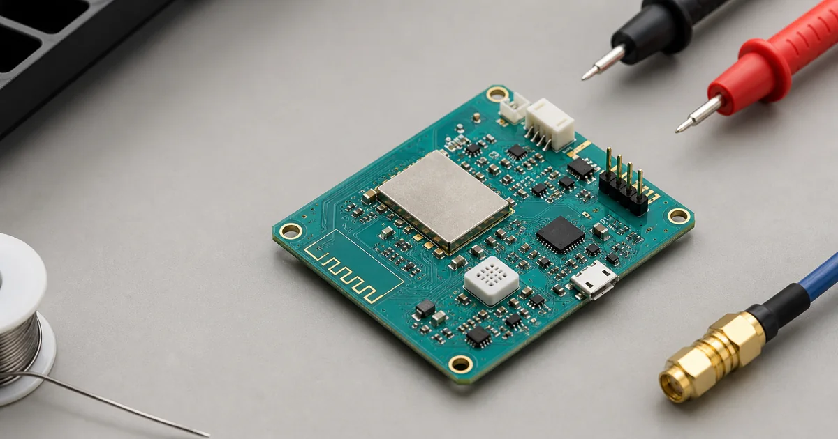
IoT sensor assembly risk often comes from interactions between the wireless module, antenna region, sensor interfaces, power architecture, firmware and enclosure rather than component placement alone. Use the module and sensor manufacturers' current hardware guidance, then define programming and test evidence for the actual product state.
IoT Sensor PCB Review Checklist
| Dimension | Review question | What to provide | Typical hold condition |
|---|---|---|---|
| Connectivity | Which radio, band, antenna path and keep-out rules apply? | Module/device reference design and antenna documentation | Layout differs from mandatory guidance without RF review |
| Modules | Does the exact module variant match footprint, certification assumptions and firmware? | Exact MPN, datasheet and hardware revision | BOM names a family rather than an orderable variant |
| Sensors | Are supply, interface, address, orientation and environmental exposure defined? | Datasheets, schematic and calibration/test notes | Sensor behavior cannot be linked to a test condition |
| Power | What are startup, sleep, transmit and peak-current states? | Rail limits, sequencing and expected current states | The test supply cannot reproduce required states |
| Interfaces | Which connectors, buses, levels and debug paths must be accessible? | Pinout, cable/fixture information and protection notes | Programming or debug access is blocked |
| Component lifecycle | Are wireless modules and sensors available for follow-on builds? | Lifecycle status, approved alternates and ownership | A constrained module has no decision path |
| Programming | Which bootloader, application image, keys and identifiers belong to the board revision? | Released binaries, procedure and serialization rules | Firmware and hardware revisions are not mapped |
| Testing | Which power, sensor, connectivity and interface behaviors must pass? | Procedure, limits, fixtures and retained evidence | Pass/fail is described only as powers on |
| Mechanical integration | Does the enclosure affect antenna, sensors, connectors or calibration? | Mechanical context and assembled-product test plan | Board-only evidence is treated as product-level validation |
Wireless module and antenna review
Module-specific layout guidance can require an antenna keep-out, ground-plane conditions, matching networks or a defined RF test connector. These requirements are not interchangeable between products. Use the exact module/device documentation and review any departure before committing the PCB revision.
Power and sensor behavior
A current measurement at idle is not enough when the product has startup, transmit, acquisition, sleep or sensor-heater states. Define the state, supply conditions, expected range and timing. For GNSS modules, clean supply and antenna implementation can affect acquisition behavior; for battery products, programming and test fixtures must avoid hiding power-state faults.
Programming and validation package
- Map hardware revision, module variant and firmware image.
- Define provisioning, keys, serial identifiers and data ownership when applicable.
- Provide interface commands, expected sensor values and tolerances for the test condition.
- Separate board-level connectivity checks from enclosure-level RF and product validation.
- Record failures by unit, revision, firmware and disposition.
Technical sources
Continue the decision path
Continue with the related service and engineering guides for the current build stage.
Need a project-specific review?
Share the released files, BOM, quantity, open decisions and required verification scope.