
PCB Assembly Testing Methods: What Each Method Can Check
Choose inspection and test coverage from the defect question, physical access, volume, setup effort and evidence required for release.
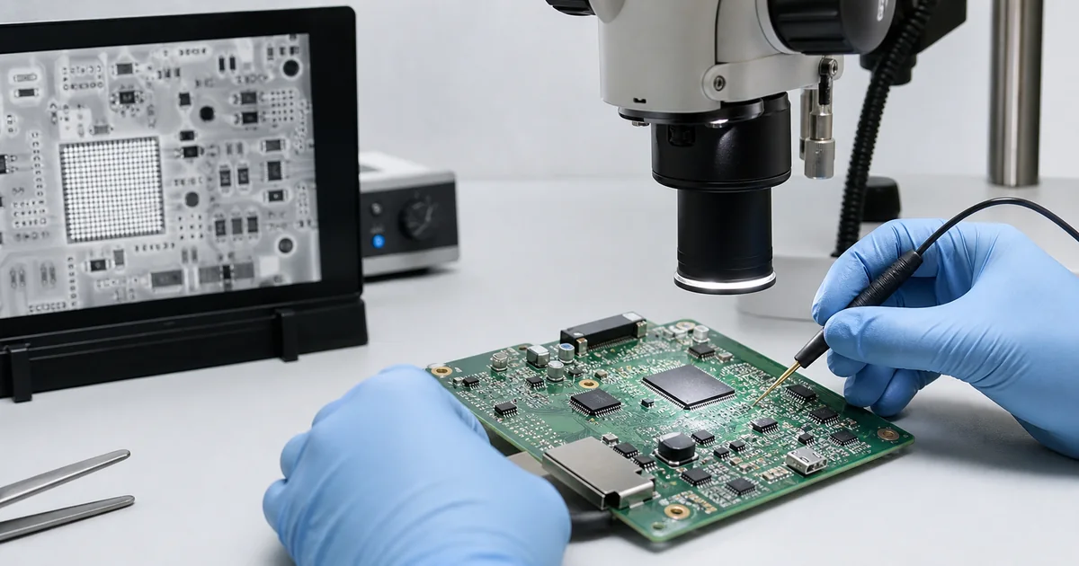
PCB assembly testing is layered. Visual inspection, AOI and X-ray look for different physical conditions; flying probe and ICT check accessible electrical nodes; programming verification confirms the intended image; functional testing checks defined product behavior. No single method proves workmanship, connectivity and function at once.
What does PCB assembly testing include?
A practical plan separates inspection from electrical and functional evidence. The sequence may include incoming data checks, visible workmanship inspection, hidden-joint imaging, connectivity measurements, programming and a customer-defined functional procedure. The selected methods depend on board access, package types, quantity and the acceptance question.
PCB Assembly Testing Decision Table
| Method | What it can check | What it needs | Important limitation |
|---|---|---|---|
| Visual inspection | Identity, orientation, polarity, visible solder conditions and obvious damage | Assembly drawing, reference sample or acceptance criteria | Cannot see hidden joints or prove electrical function |
| AOI | Repeatable optical checks for visible placement and solder features | Programmed coverage and interpretable criteria | Image results do not prove net connectivity or product behavior |
| X-ray / AXI | Hidden joints, voiding patterns and internal features that are not optically visible | Package-specific image interpretation and acceptance criteria | An image alone does not prove circuit function |
| Flying probe | Accessible nets, opens, shorts and selected component measurements without a dedicated fixture | CAD/net data, accessible targets and a test program | Coverage and cycle time depend on access and board complexity |
| ICT / bed-of-nails | Parallel access to many defined nodes for opens, shorts and component-level checks | Designed testpoints, net data and a dedicated fixture | Fixture effort is difficult to justify for unstable revisions or very small runs |
| Programming verification | Firmware image identity, programming completion and agreed read-back evidence | Released binary, interface, power sequence and revision mapping | Successful programming does not prove complete product function |
| Functional testing | Defined interfaces, loads, sensors and product behavior | Procedure, fixtures, firmware, expected results and limits | Only covers the behaviors and conditions included in the test |
How should an assembled PCB testing procedure be planned?
- Name the defect or product behavior each step is intended to detect.
- Map each method to accessible pads, connectors, interfaces or fixtures before release.
- Identify who supplies firmware, cables, fixtures, loads and golden references.
- Define pass/fail limits and the evidence that should be retained.
- Specify failure disposition, retest rules and approval ownership.
Bed-of-nails or flying probe?
Bed-of-nails ICT uses a dedicated fixture to contact many testpoints in parallel. Flying probe moves probes between accessible targets and avoids a dedicated fixture, but coverage and cycle time still depend on test access and program quality. Stable, repeated builds may justify fixture effort; early prototypes often favor flexible access and targeted functional evidence.
Required inspection and test methods, coverage, evidence, and the selected manufacturing partner's capability must be confirmed in the quotation.
Technical sources
Continue the decision path
Continue with the related service and engineering guides for the current build stage.
Need a project-specific review?
Share the released files, BOM, quantity, open decisions and required verification scope.