
PCB Assembly for IoT Devices
Route connected sensors, modules and gateways to the right prototype, sourcing, low-volume and verification path.
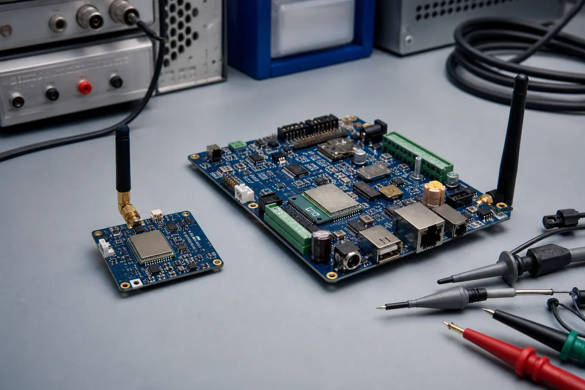
IoT PCB assembly connects the released board data with wireless-module integration, sensor and power requirements, component sourcing, programming and customer-defined validation. The assembler cannot infer antenna, firmware, enclosure or product-level compliance requirements; those decisions must be supplied and reviewed for the actual device.
Typical IoT assembly requests include wireless sensor nodes, gateway or controller boards, and designs that integrate Zigbee or other radio modules. The relevant module, antenna, firmware and validation inputs still depend on the released product design.
What makes IoT PCB assembly different?
IoT boards combine ordinary assembly requirements with interactions between RF layout, modules, sensors, power states, firmware, interfaces and an enclosure. A board can be assembled correctly yet still fail a connectivity or battery-life objective, so board-level acceptance and product validation must remain separate.
IoT PCB Assembly Review Framework
| Dimension | Question to resolve | Manufacturing input |
|---|---|---|
| Connectivity | Which radio, band, antenna implementation and RF evidence apply? | Exact module/device reference and layout guidance |
| Modules | Which orderable module variant and footprint are released? | MPN, datasheet, lifecycle and approved alternatives |
| Sensors | How do orientation, exposure, calibration and interfaces affect assembly? | Sensor notes, drawing and validation procedure |
| Power | Which startup, transmit, sleep and peak-current states matter? | Power limits, sequencing and expected measurements |
| Interfaces | Which connectors, buses, debug and programming paths must remain accessible? | Pinout, cables, fixtures and protection notes |
| Component lifecycle | Can constrained modules and sensors support the next build? | Availability review and approval ownership |
| Programming | How are firmware, keys, identifiers and hardware revision mapped? | Released files and controlled programming instructions |
| Testing | Which board behaviors and limits must pass? | Procedure, fixtures, limits and retained evidence |
| Mechanical integration | Does the enclosure alter antenna, sensor or connector behavior? | Mechanical context and product-level test plan |
How does project stage change the service path?
| Current need | Start here | Why |
|---|---|---|
| Validate a new or revised design | Prototype PCB Assembly | Prioritize learning, file review and defined bring-up evidence |
| Repeat a controlled configuration | Low-Volume PCB Assembly | Control revision, sourcing and batch acceptance |
| Coordinate PCB, parts and assembly | Turnkey PCB Assembly | Define purchasing responsibility in one project scope |
| Work against a confirmed schedule | Quick-Turn PCB Assembly | Review the critical path across files, modules, test and capacity |
| Resolve module or sensor availability | Component Sourcing | Expose lifecycle, MOQ and substitution decisions |
What should be prepared?
- Matching Gerber, BOM, CPL and assembly drawings.
- Exact module and sensor variants with hardware design references.
- Antenna, power, connector and enclosure context.
- Released firmware, programming interface and revision mapping.
- Board-level test procedure, expected results and failure disposition.
Cyrionix coordinates manufacturing partners. Wireless, programming, inspection, testing and certification requirements are confirmed for the selected project and build package.
Continue the decision path
Use the related guides and service pages to choose the right project stage and manufacturing request.
Need a project-specific review?
Share the released files, BOM, quantity, open decisions and required verification scope.